4. Technical Basics 7 - Solid State Devices
4.34 Solid state devices
- Understand that doping (adding impurities) semiconductor material (silicon and germanium) produces P-type (electron deficient) and N-type (electron rich) semiconductors.
- Understand current flow in terms of electron and hole movement.
- Understand how the P-N junction forms a semiconductor diode.
- Understand the formation and effect of the depletion layer.
- Understand the meaning of barrier potential, and forward voltage drop.
- Understand that an applied potential difference, depending on the polarity, can cause electrons to flow across the P-N junction (forward bias) or prevent electron flow (reverse bias).
Semiconductors
Before discussing the basic solid state devices used in radio and electronics work it is necessary to understand what a semiconductor is and how it is used. The term “Solid State” refers to the fact that these devices depend on the joining or fusing together of solid silicon or germanium to determine their electrical characteristics. This is a very different process from that which occurs in the thermionic valve or tube, which depends on the flow and control of a stream of electrons in a vacuum. A vacuum is an absence of all materials, solids included.
You will recall from the chapter on Ohm’s Law and DC circuits that we defined an electric current as a movement of electrons along a conductor such as a piece of copper wire. Silicon and Germanium are the two materials used in the fabrication of semiconductor devices. They are called “semi-conductor” because while in their pure state silicon and germanium are good insulators at room temperature, the addition of impurity atoms allows then to act as conductors. When a voltage is applied to them electrons are able to flow, though not as freely as in a piece of copper or gold wire.
Structure of Silicon and Germanium
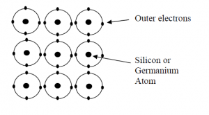
Silicon and germanium exist as a crystalline structure. Each atom has only four electrons in its outer or valence shell. It shares these electrons with each of its neighbours which also have only four electrons. This is known as co-valent bonding and it means that there are no free electrons available for conduction as there are in copper or other metals. The crystalline structure of silicon and germanium is shown below.
Changing the Conductivity
In order for silicon and germanium to be useful materials from which to make electronic devices it is necessary to enhance their conductivity. This can be achieved in two ways. Both methods involve adding impurity atoms to the pure silicon or germanium crystal. The atoms we fuse into pure silicon or germanium are known as impurities. The fusing process is known as doping.
N Type Semiconductor
If we add some atoms, such as phosphorus, that have five electrons in their outer shell to a piece of pure silicon we will have a material that has several free electrons that are able to act as current carriers. Four electrons in the outer shell of the phosphorus atom will bond with four electrons of the host silicon. The fifth electron will be free to wander through the crystal lattice and act as a current carrier.
This is known as an N-Type or electron rich semiconductor. The diagram below shows a phosphorus atom added to pure silicon. Typical doping levels can be as low as one phosphorus atom per million of silicon atoms, but this small level of impurity dramatically changes the conductivity.
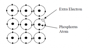
When a potential difference is applied to a piece of N Type semiconductor the free electrons, donated by the phosphorus impurity atoms, are able to flow as an electric current.
P Type Semiconductor
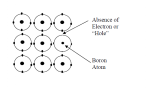
If an atom that has only three electrons in its outer shell, such as boron, is placed in the crystalline silicon there will only be three covalent bonds with the host atom. This results in the absence of one electron in the material making it P type or electron deficient. This leaves what is often referred to as a “hole” and is a difficult concept to visualize.
I will not go into detail about the nature of “holes” as it is a discipline of solid state physics in its own right. However you can think of a hole as a positive charge that is able to attract a wandering electron. If there are several holes in a piece of material electrons will be able to move through it by leap-frogging into the holes.
Again we have made it easier for electrons to move through the host material which is exactly the effect we want when we enhance the conductivity of the pure silicon or germanium.
The effect of a boron atom added to the silicon crystal is shown below.
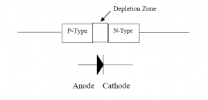
The PN Junction Diode
A PN junction diode is formed by fusing together a piece of P-Type semiconductor and a piece of N-Type semiconductor.
When the two pieces are fused together some of the electrons from the N Type fill the holes in the P Type, resulting in a small region at the junction that has no free current carriers. It is therefore known as the “depletion zone “.
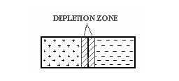
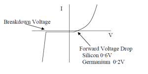
This has the effect of presenting a barrier to forward current flow through the diode of 0·6 V for silicon and 0·2 V for germanium.
This is known as the forward voltage drop of the junction, or barrier potential and is represented as Vf. The diagram below shows the structure of a PN junction diode and its circuit symbol.
Forward biasing the junction involves making the anode more positive than the cathode by 0·6V for silicon and 0·2V for germanium.
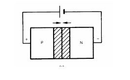
Under forward bias conditions the electrons in the N type material and the holes in the P type are repelled toward the depletion zone. When the applied voltage reaches 0∙6V for silicon and 0∙2V for germanium the depletion zone is filled and electrons are able to flow through the junction.
When the diode is reverse biased, ie the anode is negative with respect to the cathode no current can flow through the diode. The reverse bias has the effect of increasing the width of the depletion zone. If the reverse bias voltage is large enough the diode will breakdown. When breakdown occurs a heavy current can flow through the diode resulting in its destruction.
The voltage and current relationships for a junction diode are shown below.
4.35
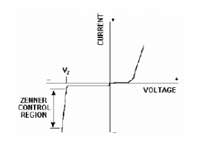
- Recall that a Zener diode will conduct when the reverse bias potential is above its designed value. Identify the E/I characteristic curve of a Zener diode.
The zener diode
A zener diode is a junction diode that is manufactured in such a way that the breakdown voltage is controlled. This allows zener diodes to be made with a range of breakdown voltages, typically from 3.3 Volts to 21 Volts. Higher voltage devices are available, up to 75 Volts, which consist of several lower voltage diodes connected in series and fabricated on one piece of material. Since the breakdown voltage is controlled, zener diodes may be used as voltage regulating devices. A typical voltage regulating circuit using a zener diode and its circuit symbol are shown below. ![]()
Note: The zener diode is operated under reverse bias conditions and that the reverse breakdown current must be limited by the series resistor R.
4.36
- Understand that the depletion layer in a reverse biased diode forms the dielectric of a capacitor and that the magnitude of the reverse bias affects the width of the layer and the capacitance.
- Understand the varactor (varicap) diode behaves as a voltage variable capacitor.
The varicap diode
The Varicap, or Varactor diode, as its name suggests is a variable capacitance diode. It too is a junction diode manufactured in such a way as to enhance its internal capacitance. Like the zener diode it is operated under reverse bias conditions.
If you think about the depletion zone that exists at the junction it is basically two conductors separated by an insulating material or dielectric. This naturally enough looks and behaves like a capacitor. As the reverse bias is increased the depletion zone widens, increasing the distance between the conducting surfaces and therefore decreasing the value of capacitance. All diodes exhibit this type of capacitance to some extent and for most applications it can adversely effect the functioning of the diode. In the Varicap however the impurity levels added to the pure silicon are adjusted to maximize the value of capacitance that exists at the junction.
As the reverse bias is increased from say 1 volt to ten volts the capacitance of the diode may change from 30 pico-Farads to 5 pico-Farads. It therefore finds use as a tuning element in resonant circuits. Changing the reverse voltage applied to the Varicap will change its capacitance and hence the resonant frequency of the circuit. The circuit symbols for the Varicap diode are shown below.
![]()
4.37
- Understand that a forward biased P-N junction emits electro-magnetic radiation and that light emitting diodes may emit infra-red or visible light.
Light emitting diodes (LED)
In any forward biased diode, free electrons cross the junction and fill the holes. When the recombination of electron/holes takes place energy is given off. In most diodes this energy is released as heat, however in an LED the energy is emitted as light. The colour of the emitted light depends on its frequency and can vary through the visible spectrum and infra red depending on material used to make the LED.
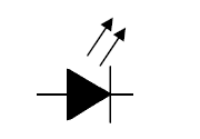
The circuit symbol for an LED is shown below
4.38
- Understand the 3 layer model of the transistor (NPN and PNP) and the channel model of the field effect transistor (FET). Understand the meaning of the term beta, or current gain of a transistor.
Transistor
Bipolar Junction Transistor ( BJT )
A bipolar junction transistor is basically two PN junctions in series
They can be manufactured from either silicon or germanium and in simple form are shown below.
![]()
The circuit symbols for NPN and PNP transistors are shown below.
![]()
The important characteristics of construction of a BJT are
The base region is very thin and lightly doped
The emitter region is heavily doped
The collector is large and usually connected to the case and/or a heat sink.
Operation of a Bipolar Transistor
Bipolar junction transistors are able to provide amplification. A small change in the current flowing through the base–emitter junction is able to control a much larger current flowing between collector and emitter.
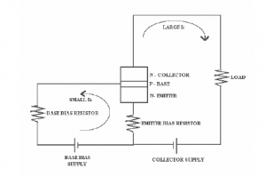
(This diagram shows separate base and collector bias supplies although in practice they are usually the same supply.)
Under normal operating conditions (that is conducting) a transistor is operated with its base–emitter junction forward biased and the collector more positive than the emitter. This results in the heavily doped emitter flooding the thin base area with charge carriers (electrons in an NPN device) to recombine with the holes in the base. Once the holes in the base are full, the electrons from the emitter are attracted to the more positive collector and current flows through the device.
There will be a 0·6V drop across the base-emitter junction for a silicon device and a 0·2 V drop for a germanium device. This is the same voltage drop that occurs across a junction diode.
A transistor can be used as a switch by biasing the base-emitter junction so in its normal state it is neutral or reverse biased so no flow occurs between the emitter and base. The switching voltage is applied to the base to cause the bias to change and bring the transistor in to a conducting state.
If a varying current is applied to the base, the biasing effect on the transistor is affected so that the conduction varies with the varying input. In this way a small input to the base can be made to control large variations at the collector, thus amplifying the input signal.
For a PNP transistor operating under normal conditions the collector will be more negative than the emitter. For both types of transistor the base–emitter junction will be forward biased.
Transistors may be used in different configurations to utilise different characteristics.
4.39
- Understand the basic methods of biasing bipolar transistors, junction FETs and MOSFETs (metal oxide semiconductor field effect transistors).
Voltage bias
Common-emitter Circuit with Voltage Divider Bias
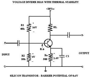
The purpose of bias in any BJT circuit is to forward bias the base emitter junction. In the circuit above this is achieved by the series circuit consisting of R1 and R2 in series with the supply voltage (+20Vcc). The NPN transistor requires the base to be positive with respect to the emitter. By applying Ohms law to R1 and R2 as a series circuit we can see that R1 will have a 16V drop across it and R2 will have 4V. Because the supply is positive the polarity’s are correct to give the base-emitter junction forward bias and leave the collector more positive than the base.
Re provides temperature stability to the circuit. As the transistor heats up the resistance between the collector and the emitter will reduce allowing more current, more heat and a thermal runaway until the transistor destroys itself.
Re has a voltage drop with its polarity in opposition to the bias voltage (which is fixed at 4V by R2). As the current through the transistor increases so the voltage drop across Re will increase effectively lowering the base-emitter bias. This reduces the collector current and controls the change in transistor output due to its heating. This process is called degeneration.
It is the DC that is flowing through Re and we are using to provide the thermal stabilisation and prevent a thermal runaway. Also within the circuit is the AC component that we are trying to amplify. The AC signal is connected to the circuit via the coupling capacitor on the input side of the circuit. If this AC signal passes through Re it will affect the bias of the transistor and reduce the gain of the transistor, defeating the purpose. A path for the AC must be provided around Re and is provided by capacitor C1 which blocks the DC forcing it through Re and allows the AC to bypass the resistor. For this to work effectively the reactance of the capacitor C1 must be about 1/10 of the value of Re, so in the above circuit the Sc of C1 would be about 50Ω. C1 is known as the emitter bypass capacitor or just the bypass capacitor while Re is the emitter stabilisation resistor.
RL is a load resistor. If it were not there the output of the transistor would be connected to the +20V DC rail and there would be no output except for the 20V DC.
The capacitors in the input and output circuits are there to contain the DC within the transistor circuit without affecting the AC which is being amplified.
You will not have to describe the complete workings of an amplifier such as this but the purpose of R1, R2, Re and C1 must be understood.
NOTE: they may be labelled differently in other diagrams.
JFET
Junction Field Effect Transistor ( JFET)
Junction field effect transistors are also able to provide amplification. These devices however operate in a different manner to BJT’s.
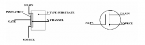
Their physical construction is shown below. Notice that these devices are manufactured using N or P type semiconductor formed as a channel in a piece of semiconductor of opposite material known as the substrate. This gives JFETS’s totally different electrical characteristics to bipolar junction transistors.
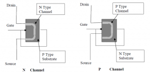
For an N Channel JFET the Gate material consists of P Type substrate. There are no P-N junctions between the source and the drain, so any supply voltage applied between source and drain will result in a current flow. No biasing is necessary to create this current flow. Since the channel is formed from N Type material there will be a depletion zone formed around/into the channel due to the same mechanism as in a junction diode. Changing the Gate Source voltage changes the width of the depletion zone and therefore that of the channel. The variation in channel width controls the current flowing between Drain and Source. If the gate voltage is sufficient the depletion zone around the channel will close the channel completely, stopping any current flow through the channel. For this reason the term cut off is not used with FETs but is replaced with the term ‘pinch off’.
The same is true for a P Channel FET but polarities are reversed.
The circuit symbols are shown below.
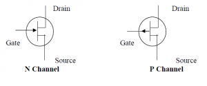
Under normal operating conditions an N-Channel FET will have its Drain at a more positive potential than its Source and its Gate voltage will be slightly more negative than its Source.
For a P-Channel device the Drain will be more negative than the Source and the Gate will be slightly more positive than the Source.
MOSFET
Metal Oxide Semiconductor Field Effect Transistor ( MOSFET)
When a FET is constructed with the gate insulated (usually with silicon dioxide) from a very narrow N channel it is known as an insulated gate FET, IGFET or MOSFET.
When a negative voltage is applied to the gate and a positive to the source, the electrostatic field from the gate extends into the N channel repelling electrons and reducing current flow. If a positive voltage is applied to the gate the drain current can be increased to a certain point (maximum flow).
With the JFET forward bias to the gate does not increase source/drain current.
Because of this the MOSFET can be operated with no bias, which simplifies circuitry.
The MOSFET has a very high input impedance (MΩ’s) and because of this static can build up on the gate to a very high voltage and rupture the insulation. Some MOSFETS are built with two zener diodes in parallel and opposite directions between the gate and the substrate to discharge any static build up. These are called gate protected MOSFETs. The symbol is the same as a MOSFET but has the zener symbols within the MOSFET symbol.
4.40
- Recall that individual components such as transistors, resistors, capacitors and diodes may be combined in packages known as integrated circuits (IC). Recall that ICs come in many forms including amplifiers, mixers and oscillators. Recall that ICs often generate heat that may need to be dissipated.
IC's
Integrated Circuits ( IC’s )
Individual components such as transistors, resistors, capacitors diodes, etc can be combined into one package known as integrated circuits. These can be produced to provide complete circuits such as amplifiers, oscillators, mixers etc contained in a single ‘chip’. The biggest problem with IC’s is the dissipation of heat away from the device. They are very often connected to heat sinks or use fans to maintain their operating temperature.